Original source: Amber Group
Original source: Amber Group
1 Introduction
Zero-knowledge proofs allow one party to prove authenticity to another party without revealing any additional information. Therefore, it can be used to protect privacy and verify the validity of transactions while hiding all details. It is important that certain zero-knowledge protocols are convenient for verifying zero-knowledge proofs, such as STARK and SNARK. These protocols generate smaller proofs, and verifying such proofs is much faster. This is well suited for resource-constrained blockchains, and is especially important in addressing scalability issues in the crypto industry. Apart from this, other use cases of zero-knowledge technology include:
DID (Decentralized ID) - to prove that an account or entity has certain"feature"feature
, such as Sismo, First Batch
Community Governance - for anonymous voting, and this use case can be extended to governance of the real world after being proven and widely adopted
Financial Statements – Entities can demonstrate compliance with certain criteria without disclosing exact financial figures
……
Cloud Service Integrity - Helping Cloud Service Providers Perform Their Missions Better
A typical zero-knowledge system
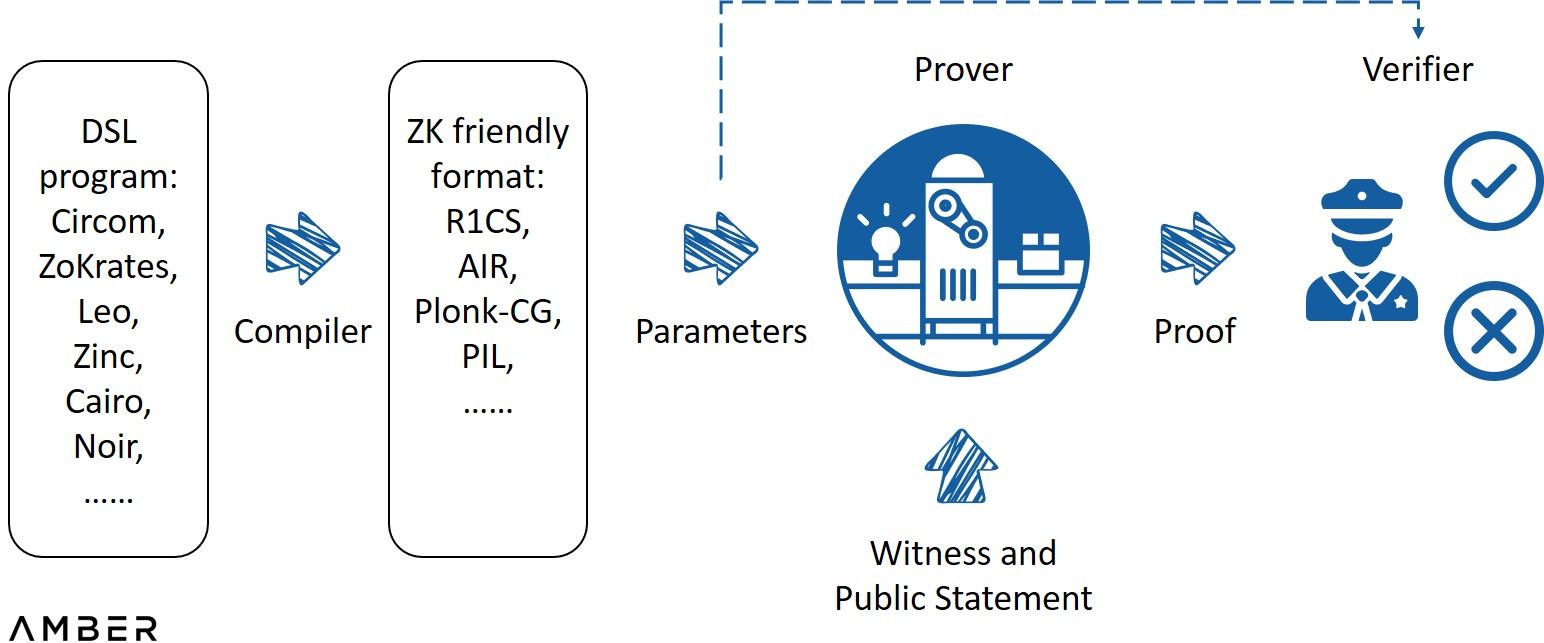
image description
Source: ZK Whiteboard Sessions - Module One, written by Prof. Dan Boneh
Several excellent proof systems have been released, such as Marlin, Plonky2, Halo2, etc. Different proof systems have different emphasis on characteristics such as the size of the generated proof, the time required for verification, and whether a trusted setup is required. After several years of exploration, it is possible to achieve constant proof size (hundreds of bytes) and short verification time (milliseconds), no matter how complex the statement is.
However, the complexity of proof generation scales almost linearly with the size of the arithmetic loop, so the difficulty may even be hundreds of times that of the original task. Since the prover at least needs to read and evaluate the loop, this can take anywhere from seconds to minutes, or even hours. The high cost of computing power and long proof time have been the main obstacles to the progress and large-scale application of zero-knowledge technology.
Hardware acceleration can help break bottlenecks. Algorithms or software optimizations are used to distribute multiple tasks to the most suitable hardware, which complement each other.
This report aims to help readers understand the market landscape, impact of zero-knowledge technology on the mining market, and potential opportunities. The report consists of three parts:
epilogue
epilogue
first level title
2. Use case
Enumerating zero-knowledge use cases will help illustrate how the market is evolving. Because different categories have different needs, hardware supply is also implicated. At the end of this section, we will also briefly compare ZKP and PoW (especially for Bitcoin).
2.1 Emerging blockchain and its differentiated requirements
The current emerging blockchains using zero-knowledge technology are the main demand side for hardware acceleration, which can be roughly divided into scaling solutions and privacy-preserving blockchains. A zero-knowledge Rollup or Volition executes the transaction off-chain and submits a succinct proof of verification via the "calldata" function. The privacy-preserving blockchain uses ZKP to allow users to ensure the validity of initiated transactions without disclosing transaction details.
These blockchains trade off properties such as proof size, verification time, and trusted settings by using different proof systems. For example, proofs generated by Plonk have constant proof size (about 400 bytes) and verification time (about 6 milliseconds), but still require a common trusted setup. In contrast, Stark does not require a trusted setup, but its proof size (~80KB) and verification time (~10ms) are suboptimal and increase with loop size. Other systems also have pros and cons. The trade-off between these proof systems will lead to a change in the "center of gravity" of the amount of computation.
Specifically, the current proof system can generally be described as PIOP (Polynomial Interactive Proof of Prophecy) + PCS (Polynomial Commitment Scheme). The former can be thought of as an agreed program used by the prover to convince the verifier, while the latter uses mathematical methods to ensure that the program cannot be broken. It's like PCS is a gun and PIOP is a bullet. The project party can modify the PIOP as needed, and can choose among different PCS.Georgios Konstantopoulos of Paradigm in hisReport on hardware acceleration
As explained in , the time required to generate a proof mainly depends on two classes of computational tasks: MSM (Multiple Scalar Multiplication Algorithm) and FFT (Fast Fourier Transform). However, instead of using fixed parameters, establishing different PIOPs and selecting from different PCSs will result in different calculations of FFT or MSM. Taking Stark as an example, the PCS used by Stark is FRI (Fast Reed-Solomon Code Proximity Interaction Proof), which is based on Liso code, rather than the elliptic curve used by KZG or IPA, so it is completely independent in the whole proof generation process. MSM is involved. We have roughly sorted the calculation amount of different proof systems in the table below. It should be noted that 1) it is difficult to estimate the exact calculation amount of the entire system; 2) the project party usually modifies the system as needed during implementation.
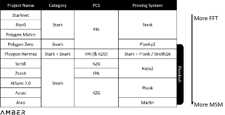
Computational Amount of Different Proof Systems
The above situation will make the project parties have their own hardware type preferences. GPUs (Graphics Processing Units) are currently the most widely used due to their large supply and ease of development. In addition, the multi-core structure of GPU is very convenient for parallel MSM computation. However, FPGAs (Field Programmable Gate Arrays) may be better at handling FFTs, which we will detail in Part II. Projects using Stark, such as Starknet and Hermez, may require FPGAs more.
Another conclusion drawn from the above is that the technology is still in its early stages and lacks standardized or dominant solutions. It may also be too early to fully use ASICs (application-specific integrated circuits) dedicated to specific algorithms. So the developers are exploring a middle ground, which we'll explain further later.
2.2 Trends and New Paradigms
2.2.1 More complex statementsDrawing on the use cases listed at the beginning, we expect zero-knowledge to have more uses in the encryption industry and the real world, and to enable more complex proofs, some of which do not even have to comply with the current proof system. Instead of using PIOP and PCS, the project party can develop new primitives that are most suitable for them. And in other fields such as MPC (secure multi-party computation), adopting zero-knowledge protocols in some works will greatly improve its utility. Ethereum recently also plans to host a Proto-DankshardingKZG Credible Setting CeremonyIn the future, we plan to further implement the full version of Danksharding to handle data availability sampling. Even Optimistic RollupIt is possible to adopt ZKP in the future
To improve security and shorten dispute processing time.While many may view zero-knowledge as a separate sector within the broad crypto industry, we believe zero-knowledge should be viewed as a technology that addresses multiple pain points in the industry.
On the other hand, in order to provide services to different systems and customers, hardware acceleration will be more flexible and versatile in the future.
. Providing a client version is a simple solution for this type of dapp, but the need to download may cause some potential users to lose, and the client is not suitable for current extension wallets or other tools.Another solution is to partially outsource proof generation. Pratyush Mishra presented during the 7th Zero Knowledge Summitthis method
Outsourced Proof Generation
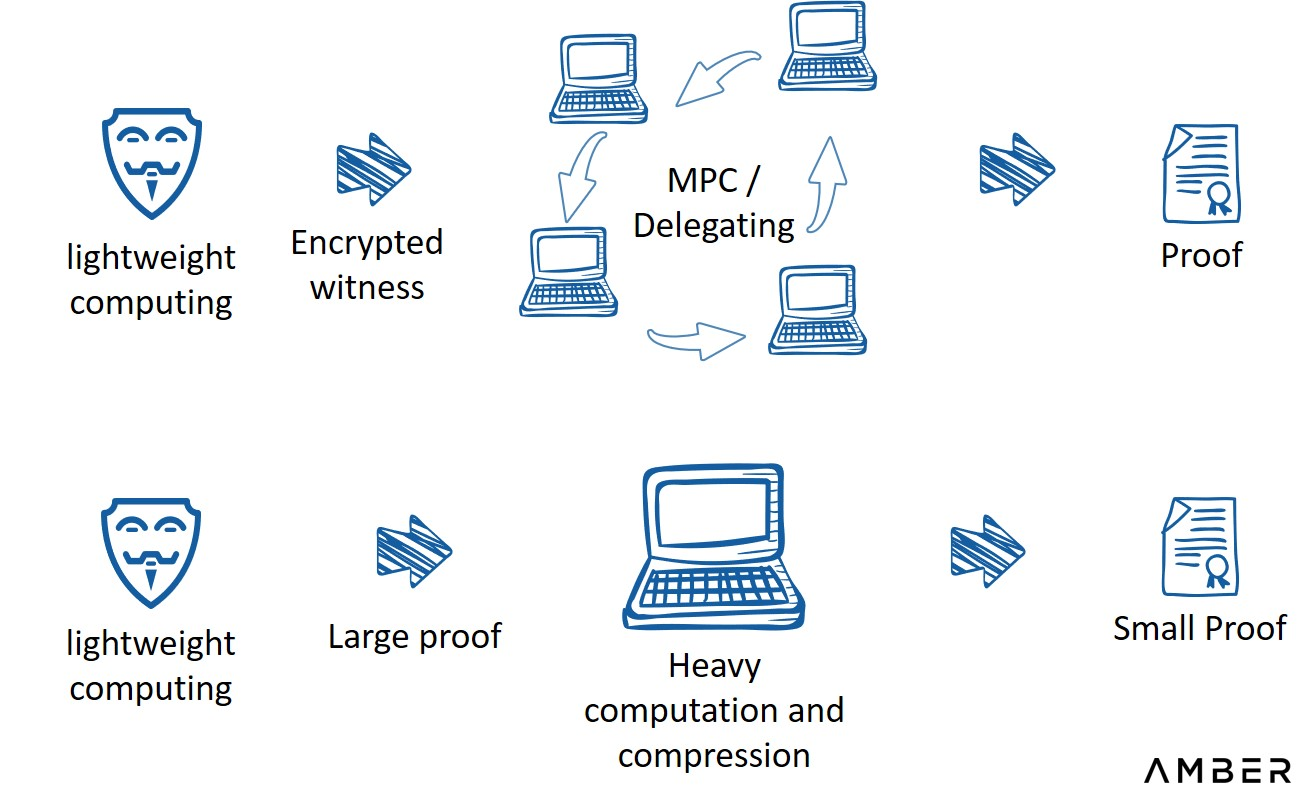
image description
Source: 7th Zero Knowledge Summit, presented by Pratyush Mishra of Aleo
2.3 Compared with PoW mining
While it would be natural to think of ZKP as a novel form of PoW and view acceleration hardware as a new type of mining machine, ZKP generation is fundamentally different from PoW mining in terms of purpose and market structure.
2.3.1 Power competition and utility calculation
Rates-are-Odds (Aleo):In order to earn block rewards and transaction fees, Bitcoin miners iterate nonces to find a small enough hash value, which is really only related to consensus. In contrast, ZKP generation is a necessary process to achieve practical utility such as information compression or privacy protection, without being responsible for consensus. This distinction affects ZKP's potentially broad participation and reward distribution model. Below we list three existing designs to illustrate how miners will coordinate ZKP generation.
Winner-Dominates(Polygon Hermez):Aleo's economic model design is the closest to that of Bitcoin and other PoW protocols. Its consensus mechanism PoSW (Concise Proof of Work) still requires miners to find an effective random value, but the verification process is mainly based on repeatedly generating SNARK proofs, which use random values and the hash value of the state root as input, and the process continues until The proof hash value generated in a certain round is small enough. We call this PoW-like mechanism the Rates-are-Odds model, because the number of verifications that can be processed in a unit of time roughly determines the probability of getting a reward. In this model, miners increase their chances of receiving rewards by hoarding large numbers of computing machines.Polygon Hermez takes a simpler model. according to thempublic document
Party-Thresholds (Scroll):From the perspective of content, the two main players are the orderer and the aggregator, the orderer collects all transactions and preprocesses them into new L2 batches, and the aggregator specifies its verification intent and competes to generate proofs. For a given batch, the first aggregator to submit a proof will earn the fee paid by the orderer. Aggregators with state-of-the-art configurations and hardware are likely to dominate regardless of geographic distribution, network conditions, and verification strategies.
Scroll describes their design as "Layer 2 proof outsourcing", where miners who stake a certain amount of cryptocurrency will be arbitrarily selected to generate proofs. The selected miners need to submit proofs within the specified time, otherwise their selection probability for the next epoch will be lowered. Generating wrong proofs will result in fines. At first, Scroll will probably work with a dozen or so miners to improve its stability, and even run its own GPU. And over time, they plan to decentralize the entire process. We use this decentralized implementation time node as a parameter to measure the adjustment of Scroll's center of gravity between efficiency and decentralization. Starkware might also fall into this category. In the long run, only machines with the ability to complete proofs in a timely manner can participate in proof generation.Each of these coordinated designs has a different focus. We expect Aleo to have the highest decentralization, Hermez to have the highest efficiency, and Scroll to have the lowest barrier to participation.
But based on the above design, a zero-knowledge hardware arms race is unlikely to happen anytime soon.
2.3.2 Static Algorithms and Evolutionary Algorithms
We believe that compared with the simple and static PoW market, the difference of ZKP contributes to a more decentralized and dynamic market structure. We propose to think of ZKP generation as a service (some startups christen it ZK-as-a-Service), where ZKP generation is a means to an end rather than an end. This new paradigm will eventually lead to new business or revenue models, which we will detail in the final section. Before that, let's take a look at multiple solutions.
first level title
3. Solutions
The CPU (central processing unit) is the main chip in a general-purpose computer, and is responsible for distributing instructions to various components on the motherboard. However, since the CPU is designed to handle multiple tasks quickly, which limits the processing speed, GPUs, FPGAs, and ASICs are often used as assistants when dealing with concurrent or certain specific tasks. In this section, we will focus on their characteristics, optimization process, status quo, and market.
3.1 GPU: Currently the most commonly used hardwarepippengerThe GPU was originally designed to manipulate computer graphics and process images, but its parallel structure makes it a good choice in fields such as computer vision, natural language processing, supercomputing, and PoW mining. GPUs can accelerate MSM and FFT, especially for MSM, by exploiting the so-called "
" algorithm, the process of developing GPU is much simpler than FPGA or ASIC.
The idea of acceleration on the GPU is very simple: offload these computationally demanding tasks from the CPU to the GPU. Engineers will rewrite these parts into CUDA or OpenCL. CUDA is a parallel computing platform and programming model developed by Nvidia for general computing on Nvidia GPUs. CUDA's competitors are heterogeneous computing developed by Apple and Khronos Group. Provides standard OpenCL, which makes users no longer limited to NVIDIA GPUs. These codes are then compiled and run directly on the GPU. For further acceleration, developers can also:
(1) To reduce data transfer costs (especially between CPU and GPU), optimize memory by using as much fast storage as possible and less slow storage.
(2) In order to improve hardware utilization and make the hardware work at full capacity as much as possible, optimize the execution configuration by better balancing the work among multi-processors, building multi-core concurrency, and reasonably allocating resources for tasks.
In short, we want to do our best to parallelize the entire work process. At the same time, the sequential execution process in which the latter item depends on the result of the former item should be avoided as much as possible.
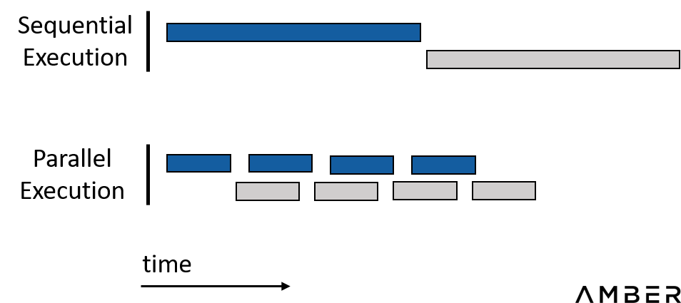
Save time with parallelization
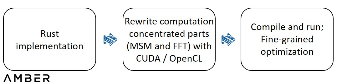
GPU Accelerated Design Flow
3.1.1 Huge developer group and development convenienceUnlike FPGAs and ASICs, GPU development does not involve hardware design. CUDA or OpenCL also has a large developer community. Developers can quickly build their own modified versions based on the open source code. For example, Filecoin released back in 2020. Supranational also recently open-sourced their general accelerationsolutionsolution
, which is probably the best open source solution of its kind at the moment.This advantage is even more pronounced when considering work beyond MSM and FFT. Proof generation is indeed dominated by these two items, but the other parts still account for about 20% (source:Sin7Y's white paper
), so only speeding up MSM and FFT has a limited effect on shortening the proof time. Even if the calculation time of these two items is compressed to an instant, the total time spent is still only one-fifth of the original time. Also, since this is an emerging and evolving framework, it is difficult to predict how this ratio will change in the future. Given that FPGAs need to be reconfigured, and ASICs may also need to be redesigned for production, GPUs are more convenient for accelerating heterogeneous computing jobs.
3.1.2 Surplus GPUs
GPU chip market share
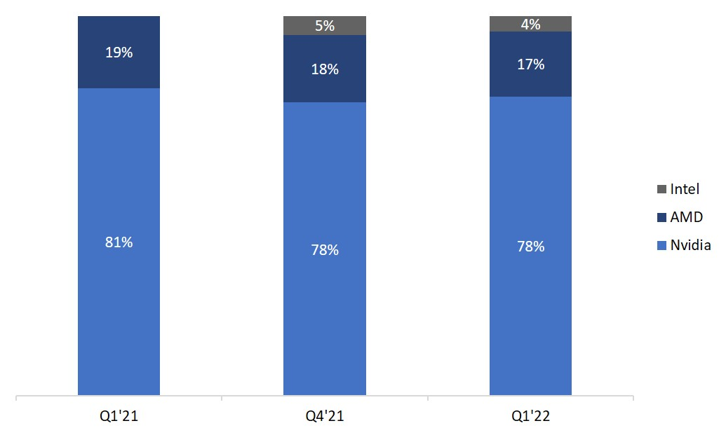
image description
Especially for mining, we conservatively estimate atethereum mergerethereum merger
Ethereum hash rate
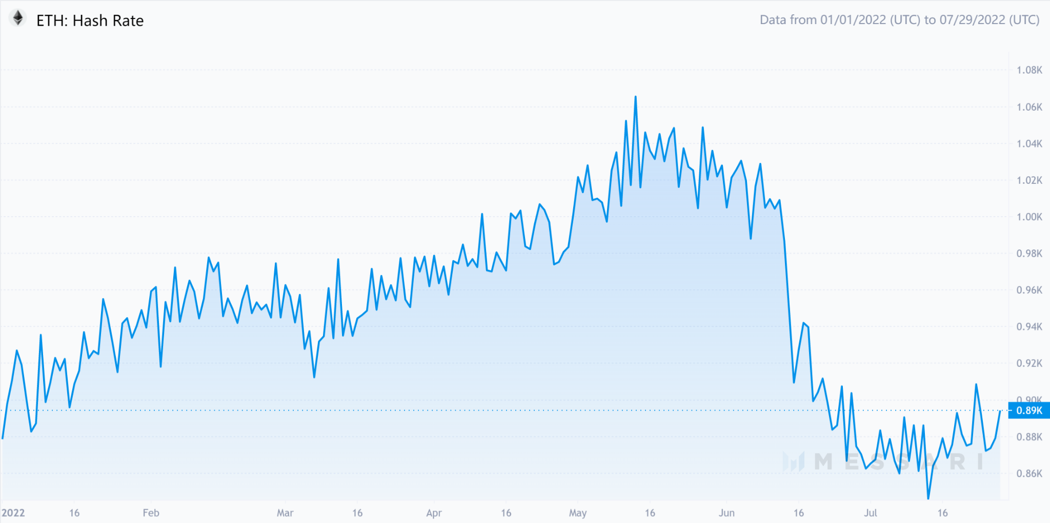
image description
Source: Messari
3.2 FPGA: Balancing Cost and Efficiency
An FPGA is an integrated circuit with a programmable structure. Because the circuitry inside the FPGA chip is not hard etched, designers can reprogram it as many times as they need to. On the one hand, this effectively cuts the high manufacturing costs of ASICs. On the other hand, the use of its hardware resources is more flexible than that of GPU, which makes FPGA have the potential of further acceleration and power saving. For example, while it is possible to implement optimized FFTs on the GPU, frequently shuffling the data results in a large amount of data transfer between the GPU and the CPU. However, the shuffling isn't completely random, and by programming intrinsic logic directly into the circuit design, FPGAs promise to perform tasks faster.
To achieve ZKP acceleration on FPGAs, several steps are still required. First, a reference implementation of a particular proof system written in C/C++ is required. Then, in order to describe digital logic circuits at a higher level, this implementation needs to be described in HDL (Hardware Description Language).
Then you need to simulate debugging to show the input and output waveforms to see if the code is running as expected. This step is the one that involves the most implementation. Engineers don't need the whole process, but just by comparing the two outputs they can identify minor errors. A synthesizer then converts the HDL into an actual circuit design with elements such as gates and flip-flops, and applies the design to device architecture and more analog analysis. Once the circuit is confirmed to function properly, a programming file is finally created and loaded into the FPGA device.
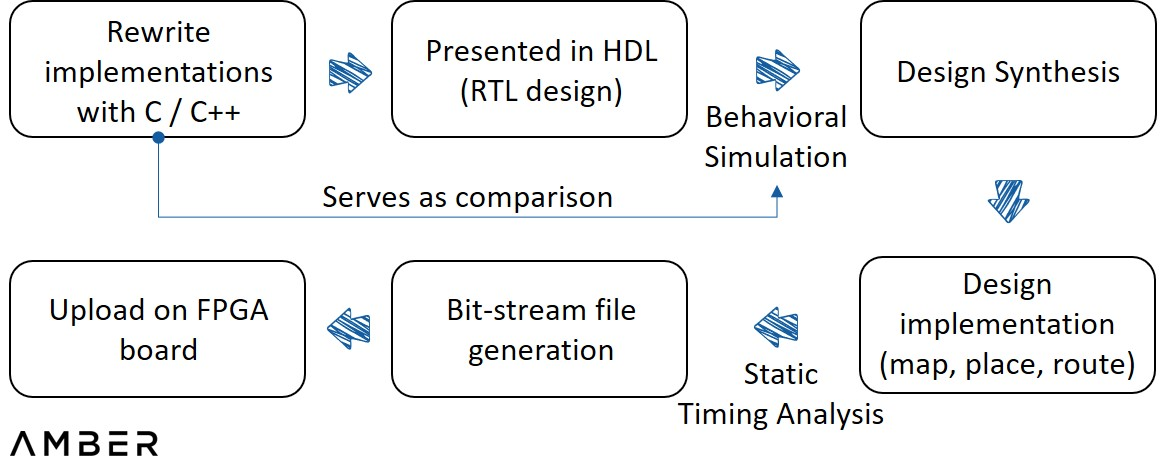
FPGA Design Flow
3.2.1 Current Barriers and Incomplete Infrastructure
Although some module optimization work on the GPU can be reused, it also faces some new challenges:
(1) For higher memory security and better cross-platform compatibility, most zero-knowledge open source implementations have been written in Rust for a long time, but most FPGA development tools are written in C/C++, which is more familiar to hardware engineers of. Teams may have to rewrite or compile these implementations before implementing them.
(2) When writing these implementations, software engineers can only choose code in a limited range of C/C++ open source libraries that can be mapped into the hardware architecture through existing development support.
(3) In addition to the work that software engineers and hardware engineers can complete independently, they also need their close cooperation to complete some in-depth optimization. For example, some modifications to the algorithm will save a lot of hardware resources while ensuring that it plays the same role as before, but this optimization is based on the understanding of hardware and software.In short, unlike AI or other mature fields, engineers must learn and build from scratch to achieve ZKP acceleration. Fortunately, we've seen more progress. For example, Ingonyama in theirrecent papers
PipeMSM is proposed in , which is a method to accelerate MSM on FPGA or ASIC.
3.2.2 Duopoly market
The FPGA market is a typical duopoly market
image description
Source: Frost & Sullivan
Engineers have realized that a single FPGA cannot provide enough hardware resources for complex ZKP generation, so multiple cards must be used simultaneously for verification. Even with a complete design, the existing standard FPGA cloud offerings from AWS and other vendors are not ideal. Additionally, startups offering acceleration solutions are often too small to have AWS or others host their custom hardware, and they don't have the resources to run their own servers. It may be a better choice to cooperate with large miners or cooperate with Web3 native cloud service providers. However, the partnership could be delicate, considering that the mining company’s in-house engineers will also likely be developing acceleration solutions.
3.3 ASIC: The ultimate weapon
ASICs are integrated circuit (IC) chips customized for specific purposes. Typically, engineers still use HDL to describe the logic of an ASIC in a manner similar to using an FPGA, but the final circuit is drawn permanently into the silicon, whereas circuits in FPGAs are made by connecting thousands of configurable blocks of. Instead of sourcing hardware from Nvidia, Intel or AMD, companies must manage the entire process themselves, from circuit design to manufacturing and testing. ASICs will be limited to certain functions, but instead give designers the greatest degree of freedom in terms of resource allocation and circuit design, so ASICs have great potential in terms of performance and energy efficiency. Designers can eliminate waste in space, power, and functionality by simply designing the exact number of doors, or sizing different modules, based on the intended application.
In terms of design process, compared with FPGA, ASIC needs to add pre-slice verification (and DFT) between the two steps of HDL writing and integration, and floorplanning is required before implementation. The former is where engineers test designs in a virtual environment using sophisticated simulation tools, and the latter is used to determine the size, shape and location of blocks in a chip. After the design is realized, all files will be sent to foundries such as TSMC or Samsung for test tape-out. If the tests are successful, the prototype is sent for assembly and testing.
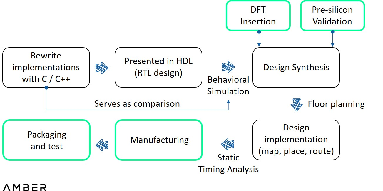
ASIC design flow
3.3.1 Relatively common ASICs in the zero-knowledge field
A common criticism of ASICs is that once the algorithm changes, previous chips are completely useless, but that doesn't have to be the case.
Coincidentally, none of the companies we spoke to planning to develop ASICs were all-in on a particular proof system or project. Instead they prefer to develop some programmable modules on the ASIC, so that different proof systems can be dealt with through these modules, and only assign the MSM and FFT tasks to the ASIC. This isn't optimal for a specific chip for a specific project, but in the short term it may be better to sacrifice performance for better generality than designing for a specific task.
3.3.1 Expensive but non-recurring costs
Not only is the design process for an ASIC much more complex than an FPGA, but the manufacturing process also consumes more time and money. Startups can contact foundries directly for tapeout or through distributors. It may take about three months or more to wait until execution actually begins. The main cost of tape-out comes from reticle and wafer. Reticles are used to create patterns on wafers, which are thin slices of silicon. Startups usually choose MPW (multi-project wafer), which can share the manufacturing cost of reticle and wafer with other project parties. However, depending on the process and the number of chips they choose, the cost of tape-out is conservatively estimated to be in the millions of dollars. Tape-out as well as assembly and testing are still several months away. If it is feasible, it will finally be able to start preparing for mass production. However, if anything goes wrong with the test, debugging and failure analysis will take an incalculable amount of time and require another tap-out. From the initial design to mass production requires tens of millions of funds, and it will take about 18 months. Take solace in the fact that a significant portion of these costs are non-recurring. In addition, ASICs have high performance and can save energy and space, which is very important, and the price may be relatively low.
Below we provide a general evaluation of different hardware solutions.
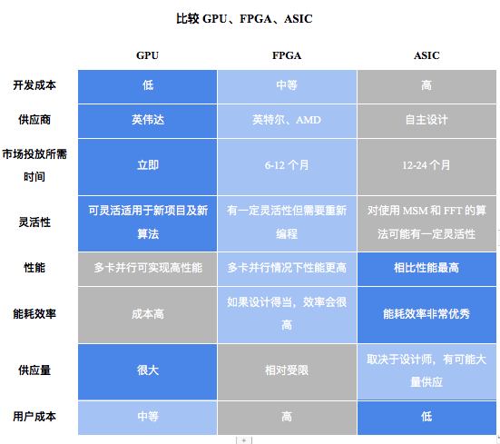
image description
Source: Amber
In order to get a more intuitive understanding of the available business models, we have shown all the potential market players in the chart below. Since there may be cross-relationships or complications between actors, we categorize them by function only.
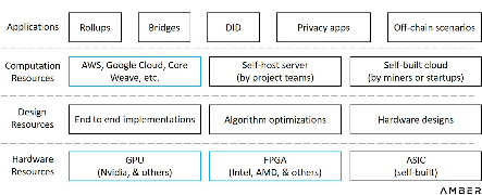
Hardware-accelerated functional layer
Zero knowledge has not yet been applied on a large scale, and building accelerated solutions will be a long process. Let's wait and see what the next turning point will be. The key question for builders and investors is when this tipping point will come.
thank you
Special thanks to Weikeng Chen (DZK), Ye Zhang (Scroll), Kelly (Supranational) and Omer (Ingonyama) for helping us understand all the technical details. Thanks are also due to Kai (ZKMatrix), Slobodan (Ponos), Elias and Chris (Inaccel), Heqing Hong (Accseal), and many others for providing insights into this research.
disclaimer
The information contained herein (“Information”) is provided for informational purposes only, in summary form and is not exhaustive. These materials are not, and are not intended to be, an offer or the solicitation of an offer to sell or buy any securities or products. Such information is not provided and should not be considered as providing investment advice. These materials do not take into account the specific investment objectives, financial situation or particular needs of any potential investor. No promises or warranties, express or implied, are made regarding the fairness, correctness, accuracy, rationality or completeness of the Materials. We make no commitment to update this material. It should not be considered by potential investors as a substitute for their own judgment or research. Potential investors should consult their own legal, regulatory, tax, business, investment, financial and accounting advisors to the extent they deem necessary, and make any investment decisions based on their own judgment and advisor's advice.